Design & enablement
From architecture and intellectual property to the tools that turn a design into manufacturable silicon.
ExploreTHE SEMICONDUCTOR PERSPECTIVE
Understand the technologies, processes and connections behind the chips that power modern life.
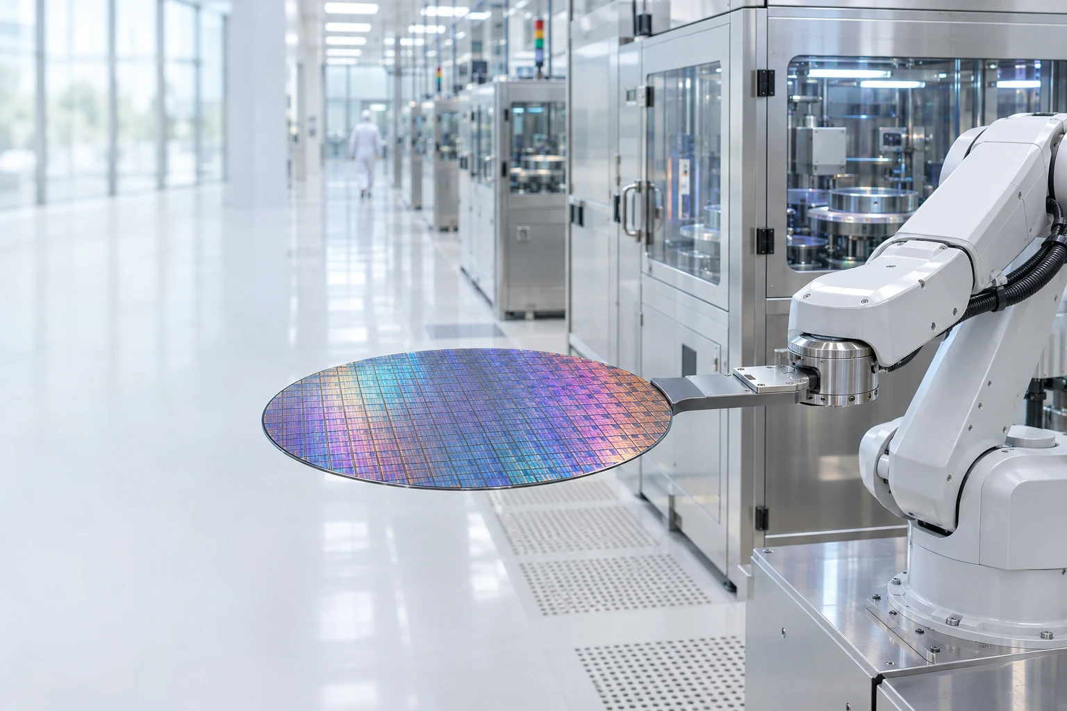
SEE THE WHOLE SYSTEM
A chip starts long before a wafer enters a fab. Explore how design, process technology and packaging work together.
From architecture and intellectual property to the tools that turn a design into manufacturable silicon.
ExploreThe repeated cycles of patterning, deposition, etch and measurement that create working devices.
ExploreConnecting dies, memory and substrates to meet a system’s performance and power requirements.
ExploreTURN ASSUMPTIONS INTO PERSPECTIVE
Explore wafer geometry, die yield and a simple cost scenario. Adjust your own inputs and see the effect.
Try the wafer plannerIllustrative model. Transparent formulas. No supplier quotes.
Higher die yield means more usable dies
from the same gross wafer count.
RESEARCH & PERSPECTIVE
2025 GLOBAL SEMICONDUCTOR SALES
US$795.6bnWSTS final annual results, released 6 March 2026.
Historical data, not a live market feed.
Why closer collaboration matters as equipment, materials and chip architectures become more interdependent.
Explore the evidenceTHE INDUSTRY ECOSYSTEM
Explore public examples across design enablement, manufacturing and equipment. Follow each entry to its original source.
Explore the ecosystemA FOUNDATION FOR WHAT COMES NEXT
Explore the platform concept, discuss its development or enquire about WorldSemiconductorCenter.com.